How Do Solar Cells Work?

Get answers to:
- What is the difference between the valence band and conduction band?
- Why are semiconductors doped?
- What is the difference between conductors, insulators, and semiconductors?
Solar cells convert light directly into electricity through some interesting atomic and quantum physics.
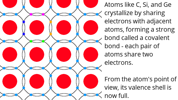
Atoms consist of a nucleus made up of protons (positively charged) and neutrons (no charge) surrounded by electrons (negatively charged). The electrons are in specific locations called shells. The outermost shell is called the valence shell. There are between one and eight electrons in this outer shell. In general, atoms combine by sharing electrons in such a way that they completely fill their valence shell.
Electricity is just the flow of free electrons – electrons which are not bound in the valence shell.
The range of energy holding the electrons in the valence shell is called the valence band. The range of energy of freely moving electrons is called the conduction band. In metals, the valence band and conduction band overlap, so electrons easily move from the valence band into the conduction band. Without an electric field to guide them, the electrons don’t move very far.
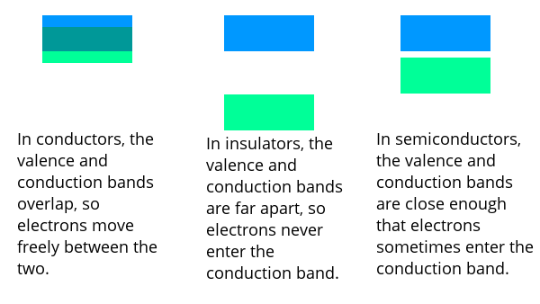
In insulators, the energy distance between the valence band and the conduction band is very large, so electrons never move from the valence band into the conduction band. Since there are no electrons in the conduction band there can be no flow of electricity.
In semiconductors, the distance between the valance band and conduction band is very small. Sometimes, electrons randomly move into the conduction band and are free to flow as electricity – if there is an electric field to move them.
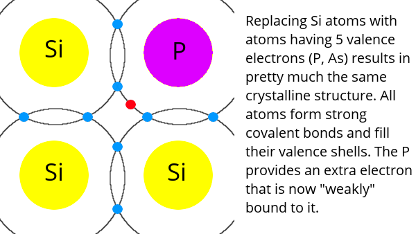
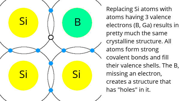
Semiconductors like silicon have four electrons in their valence shell and form crystals by sharing electrons with four neighbours – thus filling their valence shell. Pure semiconductor crystals are not very useful, so impurities are added to them. This is called doping.
Adding an element like phosphorus, which has five electrons in its valence shell, to the silicon crystal results in the extra phosphorus electron being weakly bound. This type of material is called n-type (negative-type) because it has an “excess” of electrons.
Adding an element like boron, which has three electrons in its valence shell, results in a crystal with missing electrons in the valence shell. This type of material is called p-type (positive-type) because it has an “excess” of “holes” (places where electrons can fill the valence shell).
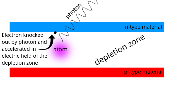
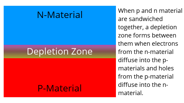
When n-type and p-type materials are sandwiched together, the “excess” electrons move to fill the holes. This creates a depletion zone. The n-side has a small positive charge (because electrons moved into the p-material) and the p-side has a small negative charge because it has an excess of electrons. This creates an electric field between the two materials – but not a flow of electricity.
When a photon with enough energy enters the depletion zone and is absorbed by an electron in a valence shell, it will knock the electron out of the valence shell and into the conduction band. At this point, the electric field between the n and p material will accelerate the electron and it will move. Moving electrons are electricity.